

Title
Real-Time Sensing with Patterned Plasmonic Substrates and a Compact Imager Chip
Document Type
Book Chapter
Abstract
Optical sensing is an important research field due to its proven ability to be extremely sensitive, nondestructive, and applicable to sensing a wide range of chemical, thermal, electric, or magnetic phenomena. Beyond traditional optical sensors that often rely on bulky setups, plasmonic nanostructures can offer many advantages based on their sensitivity, compact form, cost-effectiveness, multiplexing compatibility, and compatibility with many standard semiconductor nanofabrication techniques. In particular, plasmon-enhanced optical transmission through arrays of nanostructured holes has led to the development of a new generation of optical sensors. In this chapter we present a simple fabrication technique to use plasmonic nanostructures as compact sensors. We position the nanohole array, an LED illumination source, and a spacer layer directly on top of a standard complementary metal–oxide–semiconductor (CMOS) imager chip. This setup is a viable sensor platform in both liquid and gas environments. These devices could operate as low-cost sensors for environmental monitoring, security, food safety, or monitoring small-molecule binding to extract affinity information and binding constants.
Department(s)
Physics and Engineering
Publication Title
Biomimetic Sensing
Volume
2027
First Page
87
Last Page
100
Publication Date
1-1-2019
DOI
10.1007/978-1-4939-9616-2_8
ISSN
10643745
E-ISSN
19406029
ISBN
9781493996155
PubMed ID
31309475
Recommended Citation
Seiler, Spencer T.; Rich, Isabel S.; and Lindquist, Nathan C., "Real-Time Sensing with Patterned Plasmonic Substrates and a Compact Imager Chip" (2019). Physics and Engineering Faculty Publications. 9.
https://spark.bethel.edu/physics-faculty/9
Comments
Part of the Methods in Molecular Biology book series (MIMB,volume 2027)
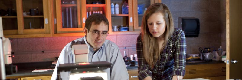
Student authors: Spencer Seiler, Isabel Rich (Physics and Engineering)
Acknowledgment: The authors thank Phil Minell and James Myrick (US Enginewing) for collaborative discussion and support. Parts of this research were also supported by the Minnesota Space Grant Consortium (MnSGC), part of the NASA-funded National Space Grant College and Fellowship Program.